
New Chip Materials: What Comes After Silicon?
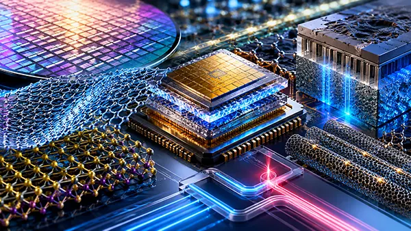
Silicon has powered modern computing for more than half a century, yet the phrase “post-silicon era” can be misleading. As of 2026, no single material is ready to replace silicon across processors, memory, communications and power electronics. Instead, the semiconductor industry is moving towards a mixed-material future. Silicon remains the main foundation because it is abundant, well understood and supported by an enormous manufacturing base, but engineers are adding new channel materials, new conductors, optical components and three-dimensional structures where silicon is no longer the best answer. The next generation of chips will therefore be defined less by one dramatic substitution and more by careful combinations: silicon nanosheet transistors for mainstream logic, atomically thin semiconductors for future scaling, silicon carbide and gallium nitride for efficient power conversion, and specialised compounds for optical or high-frequency functions. Understanding what comes after silicon means looking at which material is best suited to each part of a chip, how close it is to mass production and whether it can be manufactured reliably at an acceptable cost.
Why Silicon Is Reaching Its Limits but Will Remain Essential
The pressure on silicon comes from simple physical constraints. For decades, chipmakers improved performance by making transistors smaller and placing more of them on each chip. At very small dimensions, however, current becomes harder to control, electrical leakage increases and heat is more difficult to remove. The problem is not that silicon suddenly stops working; rather, every further improvement requires more complex structures, tighter manufacturing tolerances and higher capital spending. The smallest features named in modern process generations are no longer a direct measurement of one transistor dimension, so terms such as “2 nanometre” mainly describe a family of density and performance improvements. Even so, the engineering challenge is real. Gates, channels, contacts, insulating layers and metal wiring all have to function within spaces measured in only a few billionths of a metre, while billions of transistors must behave consistently across an entire wafer.
Silicon still has major advantages that newer materials cannot yet match. Manufacturers know how to grow high-quality silicon crystals, form exceptionally clean interfaces with silicon dioxide, control electrical behaviour through doping and produce large wafers with high yields. Design software, testing methods, factories and supply chains have also been built around complementary metal–oxide–semiconductor manufacturing. Replacing all of this would be far more difficult than demonstrating an impressive transistor in a university laboratory. Reliability is especially important: a new material must survive years of electrical stress, repeated heating and cooling, mechanical strain and manufacturing variation. It must also work in both n-type and p-type transistors, because modern logic relies on carefully balanced pairs of each. Many post-silicon candidates perform well in one narrow role but still struggle to meet this complete set of requirements.
Current production plans show how much life remains in silicon. TSMC reported that its N2 generation, based on gate-all-around nanosheet transistors, entered high-volume manufacturing in the fourth quarter of 2025 and was expected to ramp quickly during 2026. Its N2P and A16 developments, scheduled for volume production in the second half of 2026, continue to use advanced silicon transistor technology while changing power delivery and design choices. Intel’s 18A process entered production in 2025 and combines RibbonFET gate-all-around transistors with backside power delivery; in June 2026, the company said the enhanced 18A-P version had entered risk production. These developments matter because they demonstrate that the immediate successor to older silicon transistors is not a different chemical element. It is a more sophisticated form of silicon computing, with the gate wrapped around the channel and power supplied from the back of the wafer to free space for signal wiring.
From Nanosheets to Vertically Stacked Transistors
Gate-all-around transistors are the main bridge between today’s FinFETs and later mixed-material devices. In a FinFET, the gate controls a raised silicon fin from three sides. In a nanosheet design, thin horizontal sheets of channel material pass through a gate that surrounds them more completely. This stronger control helps reduce leakage and allows engineers to adjust sheet width for different performance or power targets. Leading manufacturers have now moved gate-all-around structures into their newest process generations. The important point for non-specialists is that transistor design is becoming three-dimensional at the level of the switching device itself. Engineers are no longer relying only on shrinking a flat pattern; they are changing the shape of the transistor so that electricity remains controllable as dimensions fall.
The next step is likely to place complementary transistors above one another. This idea is commonly called a complementary field-effect transistor, or CFET. Instead of positioning n-type and p-type devices side by side, manufacturers would stack them vertically, reducing the area needed for a logic cell. IBM has also described a sequentially built NanoStack architecture in which nanosheet transistor layers are bonded and processed one above another. Such designs could improve density without demanding that every horizontal feature become dramatically narrower. They also fit a broader change in chip engineering: useful progress increasingly comes from moving upwards. The difficulty is that upper layers must be added without damaging devices already completed underneath. Heat budgets, alignment, electrical connections and defect control therefore become as important as the electrical properties of the channel material.
Vertical stacking will not remove the need for new materials; it will create more places to use them. A lower transistor layer may continue to use silicon because it tolerates established high-temperature processing, while an upper layer could use a semiconductor deposited at a lower temperature. Contacts may require metals that retain low resistance at tiny dimensions, and insulating layers must prevent unwanted electrical coupling between stacked devices. Heat will also become a central constraint because densely packed layers can trap energy inside the chip. This is why the post-silicon discussion cannot be reduced to choosing a better transistor channel. A practical design must consider channels, contacts, wiring, insulation, power delivery and cooling as one connected system. The strongest candidate will be the one that improves overall computing efficiency without creating an even more serious problem elsewhere.
The Materials Most Likely to Extend or Replace Silicon in Specific Roles
Two-dimensional semiconductors are among the most closely watched candidates for future logic. Materials such as molybdenum disulphide and tungsten diselenide can be only one or a few atomic layers thick. Their thinness gives a transistor gate strong control over the channel, which could reduce leakage when devices become too small for conventional silicon channels. They also have useful electronic band gaps, unlike graphene, which conducts extremely well but does not naturally switch off in the way ordinary digital logic requires. Research reported during 2025 showed meaningful progress towards manufacturing rather than isolated laboratory demonstrations. Imec presented improved p-type transistors using monolayer tungsten diselenide, together with more factory-compatible methods for forming contacts and gate structures. Separate research demonstrated wafer-scale molybdenum disulphide transistors with channel and contact lengths below 35 nanometres and statistics gathered from roughly one thousand devices.
The appeal of two-dimensional materials is not limited to smaller individual transistors. Because they can be processed in extremely thin layers and, in some cases, at lower temperatures than traditional silicon devices, they may be well suited to building logic or memory directly above existing circuitry. In 2025, researchers reported a simple processor made from around one thousand n-type molybdenum disulphide transistors and one thousand p-type tungsten diselenide transistors on the same chip. Another project integrated a two-dimensional molybdenum disulphide memory layer with conventional CMOS control circuitry and reported a fabrication yield of about 94 per cent. These results do not mean that commercial laptop processors made entirely from two-dimensional materials are imminent. They do show that the field is moving from single-device records towards circuits, wafer-scale growth, repeatability and integration with established electronics.
Serious obstacles remain. Growing a uniform, nearly defect-free film across a large wafer is harder than producing a small high-quality flake. Electrical contacts can introduce enough resistance to cancel the benefit of an excellent channel, while suitable insulating layers do not naturally form on many two-dimensional surfaces. P-type performance has generally lagged behind n-type performance, making balanced logic more difficult. Manufacturing must also avoid contamination and must place each layer with atomic-level control. For these reasons, the first commercial use may be selective: an added layer of low-power logic, specialised memory, sensors or circuitry built above a silicon base. A full replacement of silicon in leading central processors would require advances in materials growth, contacts, gate insulation, device lifetime, circuit design and high-volume quality control at the same time.
Carbon Nanotubes, Compound Semiconductors and Wide-Bandgap Devices
Carbon nanotubes offer another route to highly efficient transistors. A nanotube is a rolled cylinder of carbon atoms with a diameter that can approach one nanometre. Semiconducting nanotubes can carry current effectively at low voltage, making them attractive for energy-efficient logic and for additional transistor layers above silicon. Research groups have already built processors and wafer-scale test circuits using carbon-nanotube field-effect transistors. The challenge is not proving that a nanotube can switch; it is arranging vast numbers of them in the correct direction, at the required density and with consistent electrical properties. A small fraction of metallic nanotubes that cannot switch off can cause circuit failures. Engineers therefore need reliable methods for growth, alignment, transfer, purification, doping and contact formation before carbon-nanotube logic can compete with mature silicon production.
Compound semiconductors combine elements from different groups of the periodic table and are already essential where silicon is less effective. Gallium arsenide and indium phosphide are widely used in radio-frequency and optical components because electrons can move through them quickly and because some compounds emit or detect light efficiently. Rather than replacing an entire silicon processor, these materials are increasingly being attached as small specialised dies. In June 2026, imec reported progress in integrating III-V chiplets with silicon CMOS through a 300-millimetre interposer designed for high-frequency and data-centre uses. This approach reflects a realistic materials strategy: keep silicon for dense digital control, then add a compound semiconductor only where its speed, optical response or high-frequency behaviour justifies the extra cost and manufacturing complexity.
Silicon carbide and gallium nitride are further ahead in power electronics. Their wide band gaps allow devices to operate at higher voltages, temperatures and switching frequencies than conventional silicon components, with lower losses in many applications. Silicon carbide is particularly important in electric-vehicle traction inverters, rapid chargers, industrial drives and high-voltage energy systems. Gallium nitride is strong in compact chargers, telecommunications equipment, solar converters, robotics and power supplies for computing hardware. Commercial expansion continued through 2025 and 2026: Infineon said its 300-millimetre gallium-nitride manufacturing work was on track, with initial customer samples planned from the fourth quarter of 2025. These materials will not replace silicon CPUs, but they are already replacing silicon in parts of the electrical system that feeds, charges and controls modern electronics.
How Mixed-Material Chips Will Be Built and Used
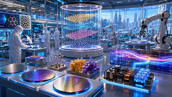
The most probable post-silicon chip is a collection of specialised parts rather than one uniform slab. Advanced packaging allows designers to divide a large design into smaller chiplets made with different processes. A computing tile can use the newest silicon transistors, memory can sit nearby on high-bandwidth stacks, analogue functions can remain on a mature and less expensive process, and optical or radio-frequency components can use a compound semiconductor. TSMC’s 3DFabric family, including CoWoS, SoIC and InFO methods, illustrates how packaging has become part of the computing architecture rather than a final protective step. Smaller dies can improve manufacturing yield, allow proven blocks to be reused and make it practical to combine materials that cannot be grown together easily on one wafer. The trade-off is that connections between chiplets must provide very high bandwidth with low energy use and dependable thermal behaviour.
Wiring inside a chip is becoming as important as the transistor material. Copper has been the standard conductor for advanced interconnects, but very narrow copper lines suffer rising resistance and require barrier layers that consume valuable space. Researchers are assessing alternatives including cobalt, ruthenium, molybdenum, topological semimetals and graphene-assisted structures. A 2025 review highlighted molybdenum phosphide and related materials as possible future conductors, graphene and molybdenum disulphide as very thin diffusion barriers, and amorphous boron nitride as a potential low-capacitance insulator. None is guaranteed to replace copper across an entire chip. More likely, different metals and barrier materials will be selected for different wiring levels, depending on line width, current, reliability and compatibility with existing production steps.
Optical communication is another major part of the mixed-material future. Moving data electrically across a package or between computing racks consumes increasing amounts of energy as AI systems grow. Silicon photonics uses familiar wafer techniques to create optical guides and many supporting components, while materials such as indium phosphide can supply lasers and compounds such as barium titanate or lithium niobate can improve light modulation. In January 2026, imec and Veeco announced a 300-millimetre-compatible method for integrating barium titanate with silicon photonics for high-speed, low-power optical functions. The likely result is not an optical replacement for every transistor. It is a closer connection between electronic logic and light-based data links, reducing the energy required to move information while silicon and other semiconductors continue to perform computation.
What the Post-Silicon Transition Will Realistically Look Like
Between 2026 and the end of the decade, most mainstream processors are expected to remain fundamentally silicon-based. Gate-all-around nanosheets, backside power delivery, improved lithography, new wiring materials and more capable packaging will provide the near-term gains. Vertically stacked complementary transistors may follow as manufacturing methods mature. Two-dimensional semiconductors and carbon nanotubes are more likely to appear first in added layers, research accelerators, sensors, memory or specialised low-power circuits than as complete replacements for leading CPUs. Compound semiconductors will continue expanding through chiplets and optical components, while silicon carbide and gallium nitride will take a larger share of power conversion. This is an incremental transition, but it is not a minor one: almost every layer of a chip and package is being reconsidered.
Cost and manufacturing yield will decide which laboratory successes become everyday products. A material may offer excellent mobility or tolerate a stronger electric field, yet still fail commercially if wafers are small, defects are common, contacts are unreliable or production requires unfamiliar equipment. Environmental and supply considerations also matter. Some compounds depend on scarce elements, energy-intensive crystal growth or supply chains concentrated in a small number of regions. Manufacturers will favour materials that can enter existing factories with limited disruption and that deliver a clear system-level benefit. This gives hybrid designs an advantage because they use small amounts of an expensive material only where it has the greatest effect, while retaining silicon for the large areas where it remains economical and dependable.
The most accurate answer to what comes after silicon is therefore “more than one material, working with silicon”. Silicon will lose its former role as the nearly universal answer to every semiconductor problem, but it will remain the structural and manufacturing centre of many advanced chips. Atomically thin channels may extend transistor scaling, carbon nanotubes may support very low-power logic, III-V compounds may handle light and high-frequency signals, silicon carbide and gallium nitride will improve power conversion, and new metals and insulators may keep data moving through increasingly dense circuits. Progress will be measured not by the day a single successor is declared, but by the gradual arrival of chips whose performance depends on several carefully integrated materials. That mixed-material approach is already visible in 2026 and is the most credible route beyond the limits of conventional silicon scaling.
Popular articles
-
 Miniature Nuclear Batteries: Can Radioisot...
A battery that keeps working for twenty, fifty or even hundreds of …
Learn more -
 Fusion Reactors with High-Temperature Supe...
Fusion energy has spent decades moving between impressive laboratory results and the …
Learn more -
 Spatial Casinos: How Mixed Reality and vis...
Casino interfaces are moving beyond flat screens. In 2026, spatial computing offers …
Learn more